(China (Mainland))

Product Summary
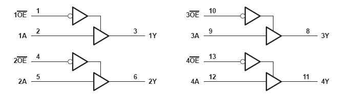
The SN74HC125DR is a quadruple bus buffer gate with 3-state outputs. The SN74HC125DR features independent line drivers with 3-state outputs. Each output is disabled when the associated output-enable (OE) input is high. To ensure the high-impedance state during power up or power down, OE should be tied to VCC through a pullup resistor; the minimum value of the resistor is determined by the current-sinking capability of the driver.
Parametrics
SN74HC125DR absolute maximum ratings: (1)Supply voltage range, VCC: -0.5V to 7V; (2)Input clamp current, IIK (VI<0 or VI>VCC): ±20mA; (3)Output clamp current, IOK (VO<0 or VO>VCC): ±20mA; (4)Continuous output current, IO (VO = 0 to VCC): ±35mA; (5)Continuous current through VCC or GND: ±70mA; (6)Package thermal impedance, θJA: 86℃/W; (7)Storage temperature range, Tstg: -65℃ to 150℃.
Features
SN74HC125DR features: (1)Wide Operating Voltage Range of 2V to 6V; (2)High-Current 3-State Outputs Interface Directly With System Bus or Can Drive Up To 15 LSTTL Loads; (3)Low Power Consumption, 80-μA Max ICC; (4)Typical tpd = 11 ns; (5)±6-mA Output Drive at 5 V; (6)Low Input Current of 1μA Max.
Diagrams
| Image | Part No | Mfg | Description |  |
Pricing (USD) |
Quantity | ||||||||||||
|---|---|---|---|---|---|---|---|---|---|---|---|---|---|---|---|---|---|---|
 |
 SN74HC125DR |
Texas Instruments |
Buffers & Line Drivers Quad Bus |
Data Sheet |
|
|
||||||||||||
|
SN74HC125DRE4 |
Texas Instruments |
Buffers & Line Drivers Quad Bus Buff Gate With 3-State Outputs |
Data Sheet |
|
|
||||||||||||
|
SN74HC125DRG4 |
Texas Instruments |
Buffers & Line Drivers QUADBusBuffer Gates |
Data Sheet |
|
|
||||||||||||