Product Summary
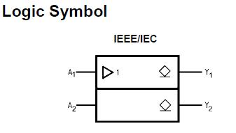
The NC7WZ07P6X is a dual buffer with open drain outputs. The NC7WZ07P6X is fabricated with advanced CMOS technology to achieve ultra high speed with high output drive while maintaining low static power dissipation over a very broad VCC operating range. The NC7WZ07P6X is specified to operate over the 1.65V to 5.5V VCC range. The inputs and outputs are high impedance when VCC is 0V. Inputs tolerate voltages up to 7V independent of VCC operating voltage.
Parametrics
NC7WZ07P6X absolute maximum ratings: (1)Supply Voltage (VCC): 0.5V to +7V; (2)DC Input Voltage (VIN): -0.5V to +7V; (3)DC Output Voltage (VOUT): -0.5V to +7V; (4)DC Input Diode Current (IIK) @ VIN <-0.5V: -50 mA; (5)DC Output Diode Current (IOK) @ VOUT < -0.5V: -50 mA; (6)DC Output Current (IOUT): +50 mA; (7)DC VCC/GND Current (ICC/IGND): ±100 mA; (8)Storage Temperature (TSTG): -65℃ to +150℃; (9)Junction Temperature under Bias (TJ): 150℃; (10)Junction Lead Temperature (TL) (Soldering, 10 seconds): 260℃; (11)Power Dissipation (PD) @ +85℃: 180 mW.
Features
NC7WZ07P6X features: (1)Space saving SC70 6-lead package; (2)Ultra small MicroPak. leadless package; (3)Ultra High Speed: tPZL 2.3 ns Typ into 50 pF at 5V VCC; (4)High IOL Output Drive: +24 mA at 3V VCC; (5)Broad VCC Operating Range: 1.65V to 5.5V; (6)Matches the performance of LCX when operated at 3.3V VCC; (7)Power down high impedance inputs/outputs; (8)Overvoltage tolerant inputs facilitate 5V to 3V translation; (9)Patented noise/EMI reduction circuitry implemented.
Diagrams

| Image | Part No | Mfg | Description |  |
Pricing (USD) |
Quantity | ||||||||||||
|---|---|---|---|---|---|---|---|---|---|---|---|---|---|---|---|---|---|---|
 |
 NC7WZ07P6X |
 Fairchild Semiconductor |
 Buffers & Line Drivers UHS Dual Buffer |
 Data Sheet |

|
|
||||||||||||
 |
 NC7WZ07P6X_Q |
 Fairchild Semiconductor |
 Buffers & Line Drivers UHS Dual Buffer |
 Data Sheet |
 Negotiable |
|
||||||||||||
 (China (Mainland))


