(China (Mainland))

Product Summary
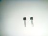
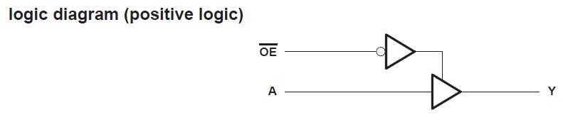
The SN74HCT125DR bus buffer gate features independent line drivers with 3-state outputs. Each output is disasbled when the associated output-enable (OE) input is high. The SN74HCT125DR is characterized for operation over the full military temperature range of –55℃ to 125℃. The SN74HCT125DR is characterized for operation from –40℃ to 85℃.
Parametrics
SN74HCT125DR absolute maximum ratings: (1)Supply voltage range, VCC: –0.5 V to 7 V; (2)Input clamp current, IIK (VI < 0 or VI > VCC): ±20 mA; (3)Output clamp current, IOK (VO < 0 or VO > VCC): ±20 mA; (4)Continuous output current, IO (VO = 0 to VCC): ±35 mA; (5)Continuous current through VCC or GND: ±70 mA; (6)Package thermal impedance, qJA: D package: 127℃/W, N package: 78℃/W; (7)Storage temperature range, Tstg: –65℃ to 150℃.
Features
SN74HCT125DR features: (1)Inputs Are TTL-Voltage Compatible; (2)High-Current 3-State Outputs Drive Bus Lines or Buffer Memory Address Registers; (3)Package Options Include Plastic Small-Outline (D) and Ceramic Flat (W) Packages, Ceramic Chip Carriers (FK), and Standard Plastic (N) and Ceramic (J) 300-mil DIPs.
Diagrams
| Image | Part No | Mfg | Description |  |
Pricing (USD) |
Quantity | ||||||||||||
|---|---|---|---|---|---|---|---|---|---|---|---|---|---|---|---|---|---|---|
 |
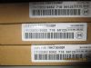
 SN74HCT125DR |
Texas Instruments |
Buffers & Line Drivers Tri-State Quad Bus |
Data Sheet |
|
|
||||||||||||
|
SN74HCT125DRE4 |
Texas Instruments |
Buffers & Line Drivers Quad Bus Buff Gate With 3-State Outputs |
Data Sheet |
|
|
||||||||||||
|
SN74HCT125DRG4 |
Texas Instruments |
Buffers & Line Drivers Quad Bus Buffer Gates |
Data Sheet |
|
|
||||||||||||