(China (Mainland))

Product Summary
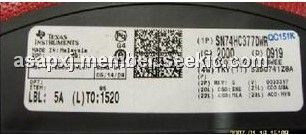
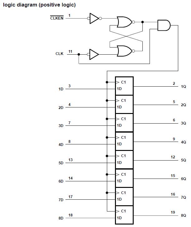
The SN74HC377DWR is a positive-edge-triggered octal D-type flip-flop with an enable input. It is similar to the ’HC273 devices, but features a latched clock-enable (CLKEN) input instead of a common clear. The SN74HC377DWR is designed to prevent false clocking by transitions at CLKEN. The applications of the SN74HC377DWR include Buffer/Storage Registers, Shift Registers, Pattern Generators.
Parametrics
SN74HC377DWR absolute maximum ratings: (1)Supply voltage range, VCC: –0.5 V to 7 V; (2)Input clamp current, IIK (VI < 0 or VI > VCC): ±20 mA; (3)Output clamp current, IOK (VO < 0 or VO > VCC): ±20 mA; (4)Continuous output current, IO (VO = 0 to VCC): ±25 mA; (5)Continuous current through VCC or GND: ±50 mA; (6)Package thermal impedance, θJA: DW package: 58℃/W, N package: 69℃/W, NS package: 60℃/W; (7)Storage temperature range, Tstg: –65℃ to 150℃.
Features
SN74HC377DWR features: (1)Wide Operating Voltage Range of 2 V to 6 V; (2)Outputs Can Drive Up To 10 LSTTL Loads; (3)Low Power Consumption, 80-μA Max ICC; (4)Typical tpd = 12 ns; (5)±4-mA Output Drive at 5 V; (6)Low Input Current of 1 μA Max; (7)Eight Flip-Flops With Single-Rail Outputs; (8)Clock Enable Latched to Avoid False Clocking.
Diagrams
| Image | Part No | Mfg | Description |  |
Pricing (USD) |
Quantity | ||||||||||||
|---|---|---|---|---|---|---|---|---|---|---|---|---|---|---|---|---|---|---|
 |
 SN74HC377DWR |
Texas Instruments |
Flip Flops Octal w/Clock Enable |
Data Sheet |
|
|
||||||||||||
|
SN74HC377DWRE4 |
Texas Instruments |
Flip Flops Octal D-Ty Flip-Flop W/Clock Enable |
Data Sheet |
|
|
||||||||||||
|
SN74HC377DWRG4 |
Texas Instruments |
Flip Flops Octal DTYPE FlipFlop |
Data Sheet |
|
|
||||||||||||