Product Summary
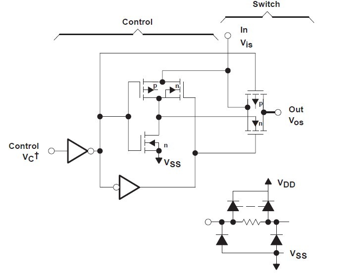
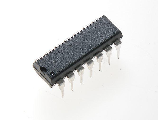
The CD4066BE is a quad bilateral switch intended for the transmission or multiplexing of analog or digital signals. The applications of the CD4066BE include: (1)Analog Signal Switching/Multiplexing: Signal Gating, Modulator, Squelch Control, Demodulator, Chopper, Commutating Switch; (2)Digital Signal Switching/Multiplexing; (3)Transmission-Gate Logic Implementation; (4)Analog-to-Digital and Digital-to-Analog Conversion; (5)Digital Control of Frequency, Impedance, Phase, and Analog-Signal Gain.
Parametrics
CD4066BE absolute maximum ratings: (1)DC supply-voltage range(VDD)voltage referenced to VSS terminal: -0.5V to +20V; (2)Input voltage range, Vis(all inputs): -0.5V to VDD +0.5V; (3)DC input current, IIN(any one input): ±10mA; (4)Package thermal impedance, θJA: E package: 80℃/W; M package: 86℃/W; NS package: 76℃/W; PW package: 113℃/W; (5)Storage temperature range(Tstg): -65℃ to +150℃.
Features
CD4066BE features: (1)15-V Digital or ±7.5-V Peak-to-Peak Switching; (2)125-Ω Typical On-State Resistance for 15-V Operation; (3)Switch On-State Resistance Matched to Within 5 Ω Over 15-V Signal-Input Range; (4)On-State Resistance Flat Over Full Peak-to-Peak Signal Range; (5)High On/Off Output-Voltage Ratio: 80 dB Typical at fis = 10 kHz, RL = 1 kΩ; (6)High Degree of Linearity: <0.5% Distortion Typical at fis = 1 kHz, Vis = 5 V p-p, VDD – VSS ≥ 10 V, RL = 10 kΩ.
Diagrams

| Image | Part No | Mfg | Description |  |
Pricing (USD) |
Quantity | ||||||||||||
|---|---|---|---|---|---|---|---|---|---|---|---|---|---|---|---|---|---|---|
 |
 CD4066BE |
 Texas Instruments |
 Analog Switch ICs Quad |
 Data Sheet |

|
|
||||||||||||
 |
 CD4066BEE4 |
 Texas Instruments |
 Analog Switch ICs Quad |
 Data Sheet |

|
|
||||||||||||
 (China (Mainland))


