Product Summary
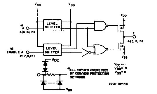
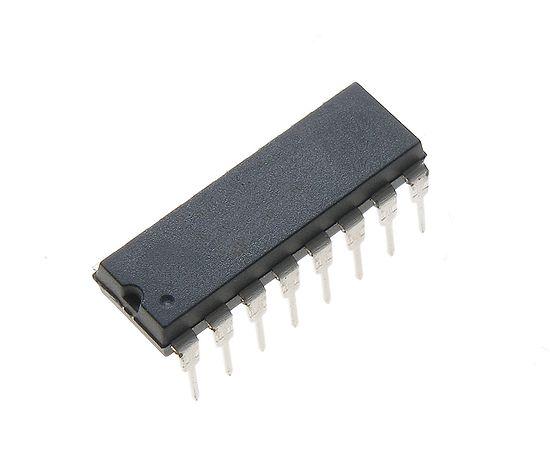
The CD40109BE is a CMOS quad low-to-high voltage level shifter. It contains four low-to-high-voltage level-shifting circuits. Each circuit will shift a low-voltage digital-logic input signal(A, B, C, D)with logical 1=VCC and logical 0=VSS to a higher-voltage out-put signal(E, F, G, H)with logival 1=VDD and logical 0=VSS. The applications of the CD40109BE include: (1)High-to-low level-shifting with three-state outputs for unidirectional or bidirectional bussing; (2)Isolation of logic subsystem using separate power supplies form supply sequencing supply loss and supply regulation considerations.
Parametrics
CD40109BE absolute maximum ratings: (1)DC supply-voltage range(VDD)voltage referenced to VSS terminal: -0.5V to +20V; (2)Output voltage range, all outputs: -0.5V to VDD +0.5V; (3)DC input current, any one input: ±10mA; (4)Power dissipation per package(PD): for TA=-55℃ to 100℃: 500mW; for TA=+100℃ to +125℃: derate linearity at 12mW/℃ to 200mW; (5)Operating-temperature range(TA): -55℃ to +125℃; (6)Lead temperature range(Tstg): -65℃ to +150℃.
Features
CD40109BE features: (1)Independence of power supply sequence considerations-VCC can exceed VDD input signals can exceed VDD input signals can exceed both VCC and VDD; (2)Up and down level-shifting capability; (3)Three-state outputs with separate enable controls; (4)Standerdized, symmetrical output characteristics; (5)100% tested for quiescent current at 20V; (6)5V, 10V and 15V perametric ratings.
Diagrams

| Image | Part No | Mfg | Description |  |
Pricing (USD) |
Quantity | ||||||||||||
|---|---|---|---|---|---|---|---|---|---|---|---|---|---|---|---|---|---|---|
 |
 CD40109BE |
 Texas Instruments |
 Translation - Voltage Levels Quad L-H Voltage |
 Data Sheet |

|
|
||||||||||||
 |
 CD40109BEE4 |
 Texas Instruments |
 Translation - Voltage Levels Quad L-H Voltage |
 Data Sheet |

|
|
||||||||||||
 (China (Mainland))


