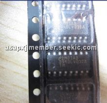
Product Summary
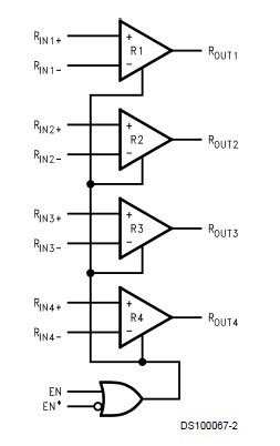
The DS90LV032ATMX is a quad CMOS differential line receiver designed for applications requiring ultra low power dissipation and high data rates. The DS90LV032ATMX is designed to support data rates in excess of 400 Mbps (200 MHz) utilizing Low Voltage Differential Signaling (LVDS) technology. The DS90LV032ATMX accepts low voltage (350 mV typical) differential input signals and translates them to 3V CMOS output levels.
Parametrics
DS90LV032ATMX absolute maxing ratings: (1)Supply Voltage (VCC): -0.3V to +4V; (2)Input Voltage (RIN+, RIN-): -0.3V to +3.9V; (3)Enable Input Voltage (EN, EN*): -0.3V to (VCC + 0.3V); (4)Output Voltage (ROUT): -0.3V to (VCC + 0.3V); (5)Maximum Package Power Dissipation +25℃: M Package: 1025 mW; MTC Package: 866 mW; Derate M Package: 8.2 mW/℃ above +25℃; Derate MTC Package: 6.9 mW/℃ above +25℃; (6)Storage Temperature Range: -65℃ to +150℃; (7)Lead Temperature Range (Soldering 4 sec.): +260℃; (8)Maximum Junction Temperature: +150℃.
Features
DS90LV032ATMX features: (1)>400 Mbps (200 MHz) switching rates; (2)0.1 ns channel-to-channel skew (typical); (3)0.1 ns differential skew (typical); (4)3.3 ns maximum propagation delay; (5)3.3V power supply design; (6)Power down high impedance on LVDS inputs; (7)Low Power design (40mW 3.3V static); (8)Interoperable with existing 5V LVDS networks; (9)Accepts small swing (350 mV typical) VID; (10)Supports open, short and terminated input fail-safe; (11)Compatible with ANSI/TIA/EIA-644; (12)Industrial temp. operating range (-40℃ to +85℃); (13)Available in SOIC and TSSOP Packaging.
Diagrams

| Image | Part No | Mfg | Description |  |
Pricing (USD) |
Quantity | ||||||||||||
|---|---|---|---|---|---|---|---|---|---|---|---|---|---|---|---|---|---|---|
 |
 DS90LV032ATMX |
 National Semiconductor (TI) |
 LVDS Interface IC |
 Data Sheet |

|
|
||||||||||||
 |
 DS90LV032ATMX/NOPB |
 National Semiconductor (TI) |
 LVDS Interface IC |
 Data Sheet |

|
|
||||||||||||
 (China (Mainland))


