Product Summary
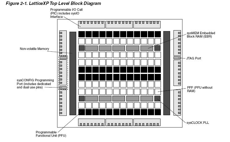
The LFXP10C-3FN256C is an award-winning DC/DC converter. The LFXP10C-3FN256C device combines logic gates, embedded memory and high performance I/Os in a single architecture that is both non-volatile and infinitely reconfigurable to support cost-effective system designs.
Parametrics
LFXP10C-3FN256C absolute maximum ratings: (1)Supply Voltage VCC: -0.5V to 3.75V; (2)Supply Voltage VCCP: -0.5V to 3.75V; (3)Supply Voltage VCCAUX: -0.5V to 3.75V; (4)Supply Voltage VCCJ: -0.5V to 3.75V; (5)Output Supply Voltage VCCIO: -0.5V to 3.75V; (6)I/O Tristate Voltage Applied5: -0.5V to 3.75V; (7)Dedicated Input Voltage Applied: -0.5V to 4.25V; (8)Storage Temperature (Ambient): -65℃ to 150℃; (9)Junction Temp(Tj): +125℃.
Features
LFXP10C-3FN256C absolute maximum ratings: (1)Non-volatile, Infinitely Reconfigurable: Instant-on–powers up in microseconds; No external configuration memory; Excellent design security, no bit stream to intercept; Reconfigure SRAM based logic in milliseconds; SRAM and non-volatile memory programmable through system configuration and JTAG ports; (2)Sleep Mode: Allows up to 1000x static current reduction; (3)TransFR. Reconfiguration (TFR): In-field logic update while system operates; (4)Extensive Density and Package Options: 3.1K to 19.7K LUT4s; 62 to 340 I/Os; Density migration supported; (5)Embedded and Distributed Memory: 54 Kbits to 396 Kbits sysMEM Embedded Block RAM; Up to 79 Kbits distributed RAM; Flexible memory resources: Distributed and block memory; (6)Flexible I/O Buffer: Programmable sysIO buffer supports wide range of interfaces: LVCMOS 3.3/2.5/1.8/1.5/1.2; LVTTL; SSTL 18 Class I; SSTL 3/2 Class I, II; HSTL15 Class I, III; HSTL 18 Class I, II, III; PCI; LVDS, Bus-LVDS, LVPECL, RSDS; (7)Dedicated DDR Memory Support: Implements interface up to DDR333 (166MHz); (8)sysCLOCK. PLLs: Up to 4 analog PLLs per device; Clock multiply, divide and phase shifting; (9) System Level Support: IEEE Standard 1149.1 Boundary Scan, plus; (10) ispTRACY internal logic analyzer capability; Onboard oscillator for configuration; Devices operate with 3.3V, 2.5V, 1.8V or 1.2V; (11) power supply.
Diagrams

| Image | Part No | Mfg | Description |  |
Pricing (USD) |
Quantity | ||||||||||
|---|---|---|---|---|---|---|---|---|---|---|---|---|---|---|---|---|
 |
 LFXP10C-3FN256C |
 Lattice |
 FPGA - Field Programmable Gate Array 9.7K LUTS 188 I/O |
 Data Sheet |

|
|
||||||||||
| Image | Part No | Mfg | Description |  |
Pricing (USD) |
Quantity | ||||||||||
 |
 LFXP10C-3F256I |
 Lattice |
 FPGA - Field Programmable Gate Array 9.7K LUTs 188 IO 1.8 /2.5/3.3V -3 Spd I |
 Data Sheet |

|
|
||||||||||
 |
 LFXP10C-3F256IES |
 Lattice |
 FPGA - Field Programmable Gate Array |
 Data Sheet |
 Negotiable |
|
||||||||||
 |
 LFXP10C-3F388CES |
 Lattice |
 FPGA - Field Programmable Gate Array |
 Data Sheet |
 Negotiable |
|
||||||||||
 |
 LFXP10C-3F388I |
 Lattice |
 FPGA - Field Programmable Gate Array 9.7K LUTs 244 IO 1.8 /2.5/3.3V -3 Spd I |
 Data Sheet |

|
|
||||||||||
 |
 LFXP10C-3F388IES |
 Lattice |
 FPGA - Field Programmable Gate Array |
 Data Sheet |
 Negotiable |
|
||||||||||
 |
 LFXP10C-3FN256C |
 Lattice |
 FPGA - Field Programmable Gate Array 9.7K LUTS 188 I/O |
 Data Sheet |

|
|
||||||||||
 (China (Mainland))


